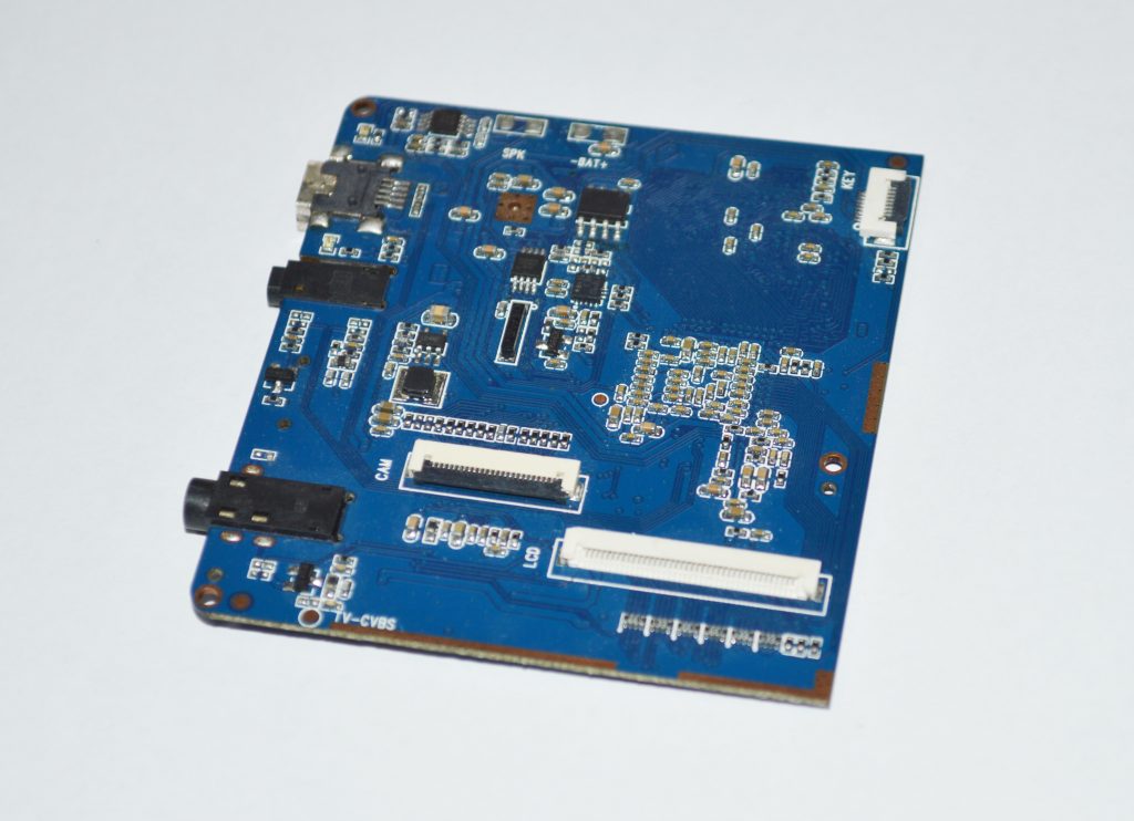
The demand for more complex and customized electronic products is growing rapidly, placing pressure on the Printed Circuit Board Assembly (PCBA) industry to improve efficiency, reduce costs, and maintain the highest standards of quality. While PCBA manufacturing is known for its intricate processes and high precision requirements, Artificial Intelligence (AI) is emerging as a powerful solution to these challenges.
From optimizing routing and placement to enhancing signal integrity, AI is transforming how PCBA designs are created, tested, and produced. Here’s how AI is shaping the future of PCBA design.

1. Optimizing Routing with AI
Routing and component placement take up a significant portion of both time and cost during the PCBA design process. AI is changing that by automating these steps, using machine learning (ML) algorithms to predict and adjust designs in real-time. This helps avoid routing congestion and interference early in the design phase.
AI tools are now able to recommend the best placement and routing options, improving the overall design quality. The result is faster turnaround times, reduced costs, and fewer errors – all of which contribute to a more efficient production process.
2. Improving Signal Integrity with AI
Signal integrity (SI) is a critical factor for ensuring the proper functioning of electronic devices. However, achieving optimal SI is a complex challenge. AI is now being used to predict and resolve potential signal issues by analyzing PCB net structures and interconnect parameters.
AI techniques like neural networks and genetic algorithms can optimize designs to ensure signals maintain their integrity, reducing the need for multiple design iterations and ensuring faster time-to-market with more reliable products.
3. Combating Counterfeit Components
The PCBA industry faces a growing issue with counterfeit components, which can lead to product failures or safety concerns. AI, combined with machine learning and computer vision, is improving the way manufacturers detect counterfeit or defective components.
By automating inspections, AI ensures that only authentic and high-quality components are used in PCBAs. This enhances product quality, reduces errors, and speeds up the inspection process – leading to improved efficiency and more reliable products.
4. Enhancing Defect Detection
As PCBs become smaller and more complex, detecting defects such as spurs, short circuits, or open circuits is becoming more difficult. Traditional Automated Optical Inspection (AOI) systems often struggle with false positives due to lighting variations or minor inconsistencies in soldering.
AI-powered systems, especially convolutional neural networks (CNNs), are now offering more accurate defect detection. These AI tools analyze high-resolution images to identify even the smallest defects with greater precision, speeding up validation and improving overall product quality.
5. Optimizing Reflow Soldering
Reflow soldering is a key process in PCBA manufacturing, ensuring that components are securely attached to the board. However, creating the right soldering profile for each component can be tricky due to differences in thermal properties.
AI is helping by optimizing reflow soldering profiles. Through machine learning, AI can predict the ideal temperature settings and conveyor speeds for components like Ball Grid Array (BGA) packages. This not only improves solder joint strength but also ensures better overall product reliability.
6. Smarter Manufacturing with AI
AI is also making PCBA manufacturing smarter by streamlining production processes. Traditional methods often involve manual tasks that are slower and prone to errors. With AI, manufacturers can now optimize supply chain management, predict demand patterns, and automate processes like inventory management and order fulfillment.
These advancements reduce waste, lower costs, and help manufacturers respond quickly to market changes. As a result, smart manufacturing is making the entire production process more efficient and cost-effective.
7. AI as a Design Assistant
AI is transforming the design phase of PCBAs as well. By learning from past designs, AI can help engineers make faster, more informed decisions, improving the overall performance, manufacturability, and testability of new designs.
AI-powered tools can also suggest ways to optimize heat dissipation, reduce costs, and enhance product performance. By automating many aspects of the design process, AI speeds up product development and reduces reliance on manual expertise, allowing engineers to focus on innovation.
Conclusion: The Future of PCBA Design
AI is fundamentally changing how PCBA designs are conceived, manufactured, and tested. From optimizing routing and improving signal integrity to detecting counterfeit components and enhancing defect detection, AI is making the entire process faster, more accurate, and more cost-effective.
At CEN PCBA, we are embracing the power of AI to deliver better, faster, and more reliable electronic manufacturing solutions. Our AI-enhanced capabilities are helping our clients achieve their goals with greater efficiency and less risk. Ready to take your PCBA designs to the next level? Get in touch with us today to learn how we can help you optimize your design and manufacturing processes.
Comments
Post a Comment